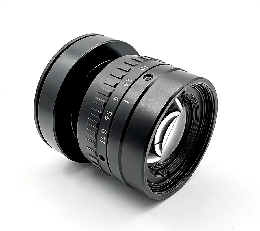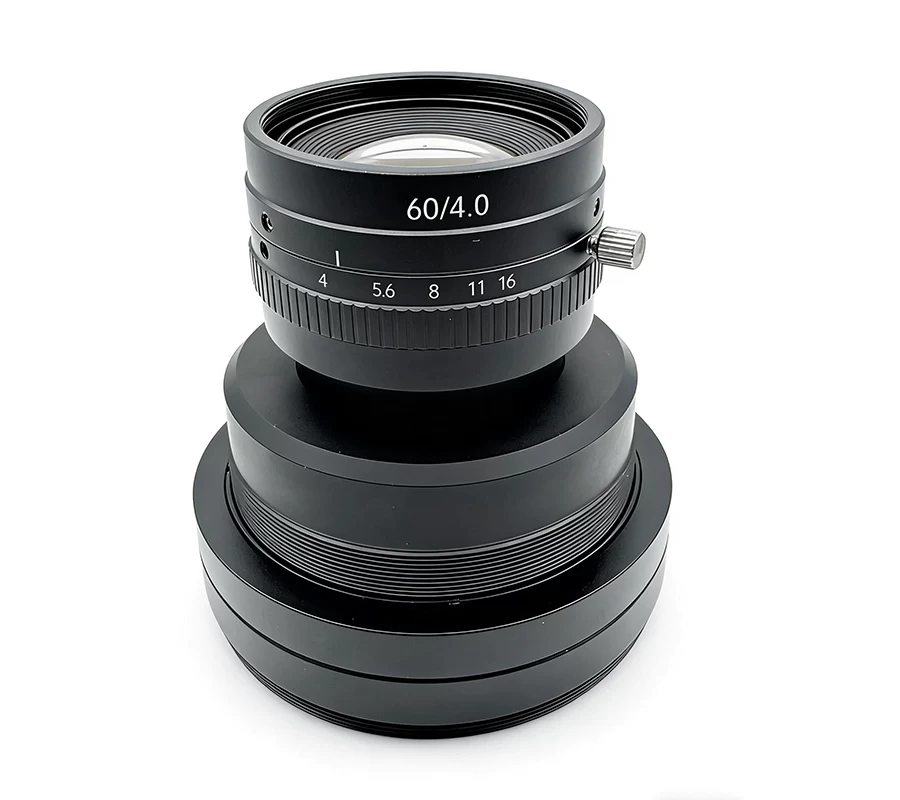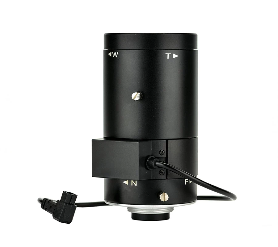
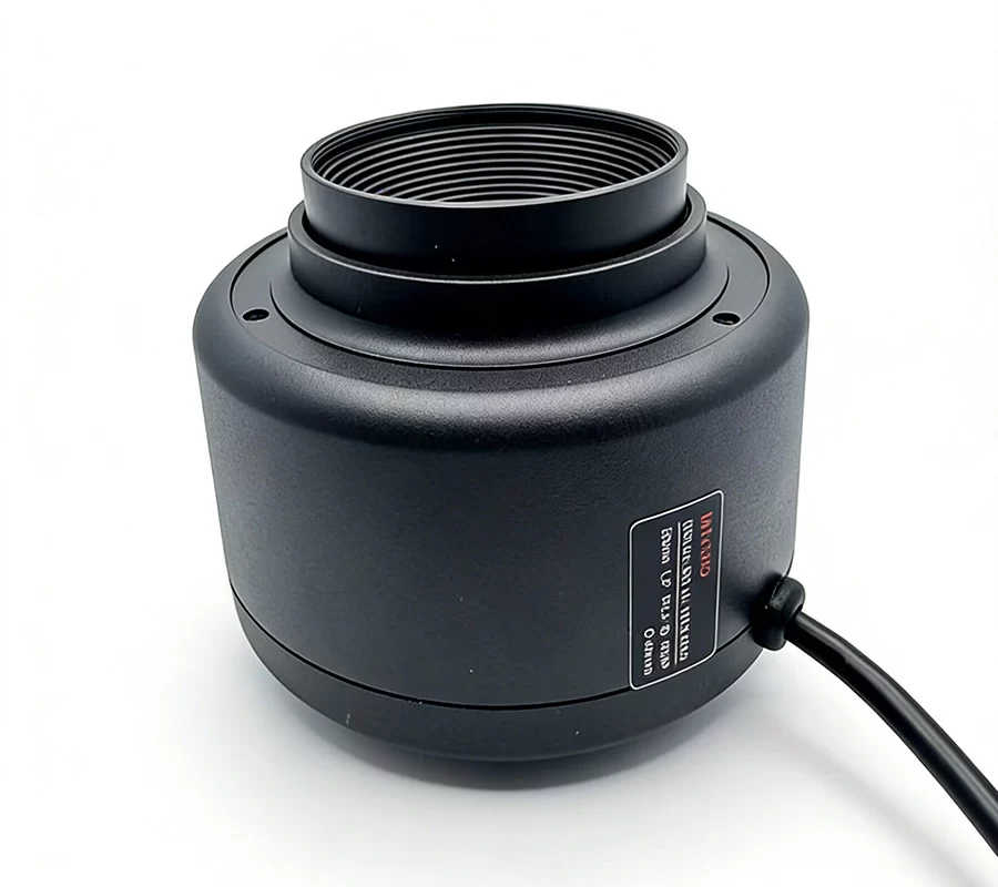
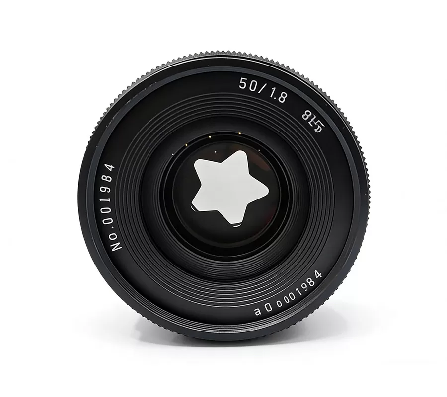
Machine Vision 35mm Lens M42/M58, Φ30 Image Circle for 4K Line Scan Camera
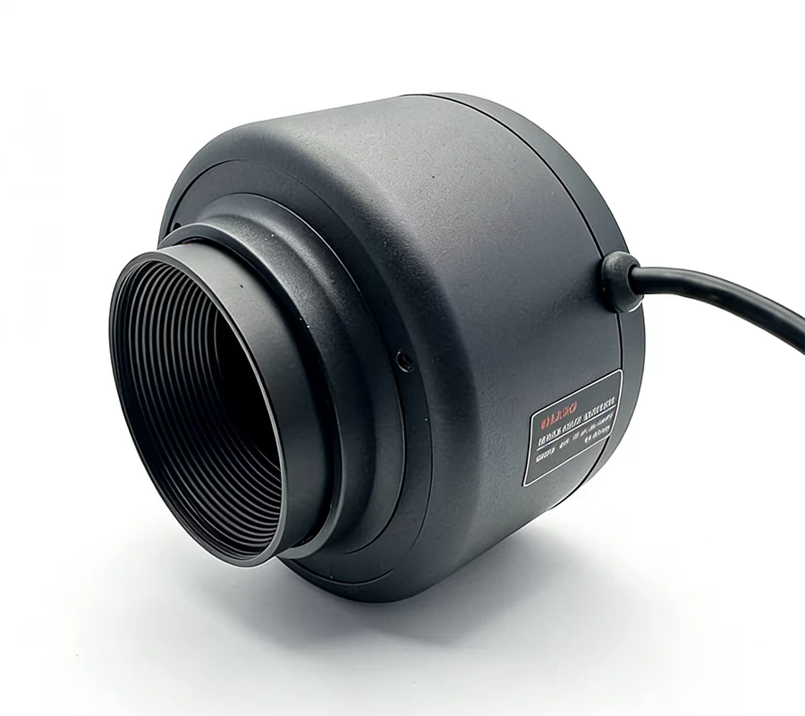
35mm Industrial Machine-Vision Lens Φ30mm Image Circle
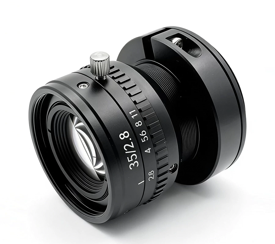
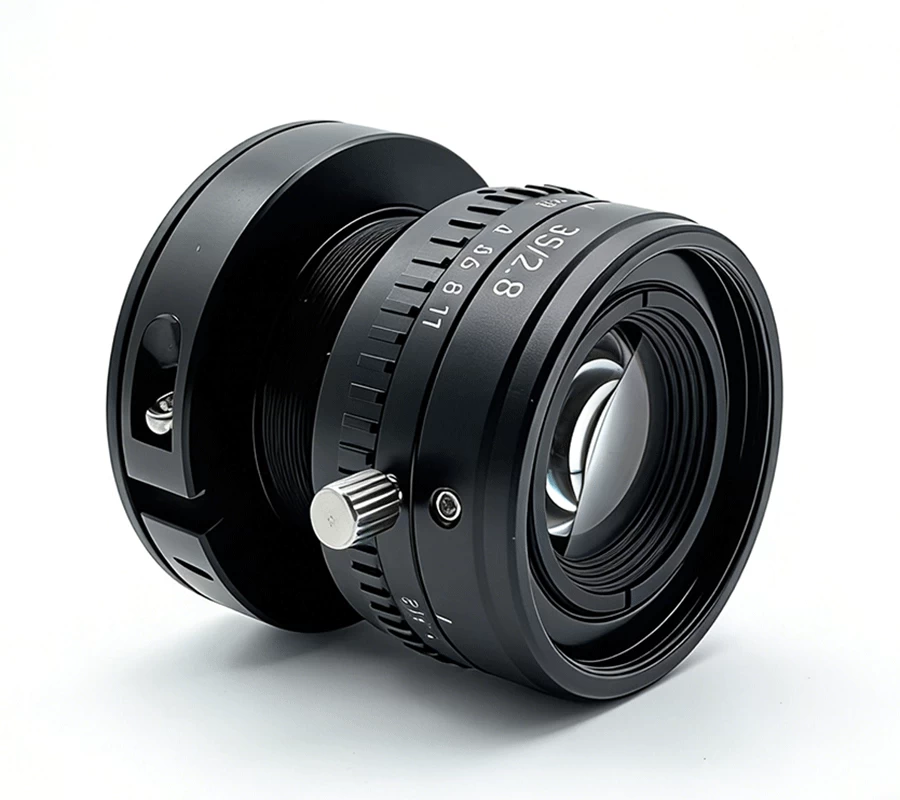
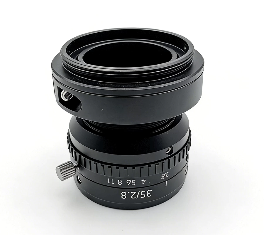
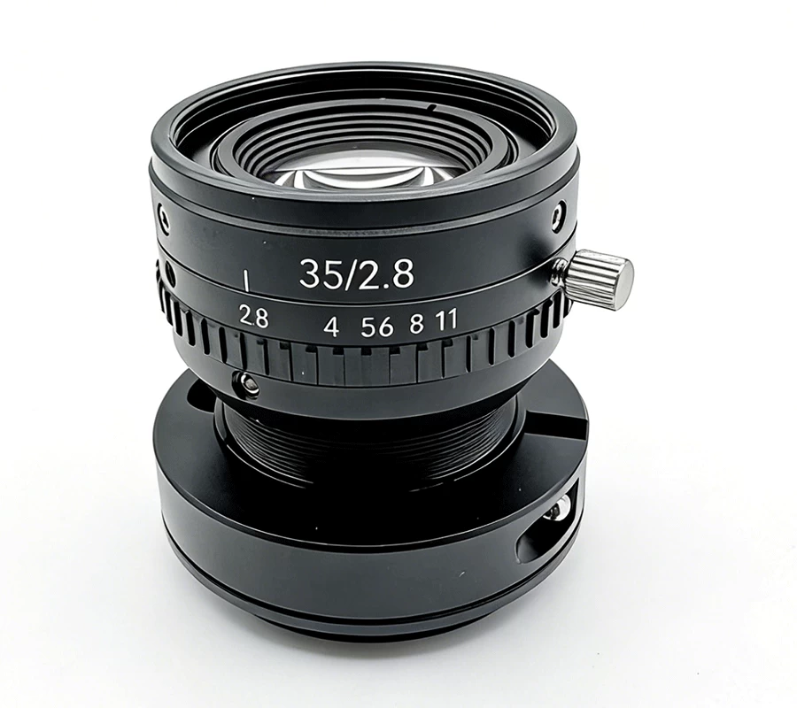
Specification of Machine Vision 35mm Lens M42/M58, Φ30 Image Circle for 4K Line Scan Camera
High-performance 35 mm fixed focal lens for 4K high-precision machine-vision systems. Optimized for Φ30 image format and 7 μm pixel sensors with ultra-low distortion for reliable metrology in harsh industrial environments.
Optical Parameters
•Resolution: 4K, compatible with 7μm pixel sensors
•Image Format: Φ30 large target surface, full imaging coverage without vignetting
•Focal Length: 35mm, balanced field of view and magnification
•Aperture: F2.8-F11 manual adjustable, suitable for low-light and high-depth-of-field scenarios
•Distortion: 0.1% ultra-low distortion, ensures high-precision measurement
•FOV: 46°, ideal for medium-distance precision inspection
•MOD: 0.2m to infinity, supports micro-detail and long-distance imaging
•BFL: Flange 12mm, Optical 21.3mm, Mechanical 12mm
•Mount: M42×1 / M58×1 optional, compatible with most industrial cameras
Application Scenarios
1. 2.5D Photometric Stereo Imaging (Core Application)
•Supports 4-channel cyclic sequential lighting (CH1→CH2→CH3→CH4) and continuous multi-angle image acquisition
•Restores micro surface topography, calculates height difference, and identifies subtle concave-convex defects invisible to 2D vision
•Widely used for 2.5D modeling and stereo inspection of precision parts, metal shells, plastic parts and glass surfaces
2. High-precision Dimension & Tolerance Inspection
•Realizes micron-level size measurement, aperture spacing and geometric tolerance detection with 0.1% ultra-low distortion
•Suitable for roundness, parallelism and verticality detection of hardware, injection molded and die-cast parts
•Applied to automatic production line size sorting and metrology quality control
3. Micro Surface Defect Detection
•Metal parts: Scratches, burrs, oxidation spots, micro cracks and polishing defects
•Plastic & silicone parts: Shrinkage, material shortage, bubbles, edge burrs and surface dirt
•Glass & lens products: Edge chipping, coating unevenness, scratches and light transmission defects
4. PCB & Electronic Component Inspection
•PCB boards: Circuit deviation, copper foil missing, soldering defects and surface scratches
•Micro components: Chip damage, pin deformation and blurred printing inspection
•Connectors & terminals: Flatness, spacing and bending defect screening
5. Automatic Production Line On-line QC
•Stable high-speed continuous shooting without ghosting, suitable for mass product rapid inspection
•Used for appearance full inspection, defect sorting, direction identification and assembly detection
6. Scientific Research & Algorithm Development
•Machine vision algorithm verification, photometric stereo algorithm training and optical imaging experiments
•3D vision modeling and multi-light sequential imaging research
7. Multi-camera Array Equipment Integration
•Lightweight and compact, convenient for multi-lens layout of 3D vision and omnidirectional scanning equipment
•Consistent imaging quality ensures overall detection accuracy of integrated equipment