High-Resolution Line Scan Lens for 16K 3.5μm Line-scan Camera
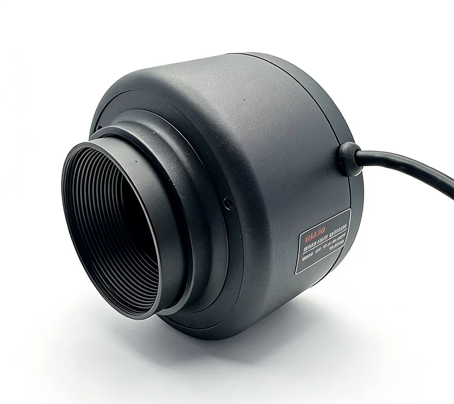
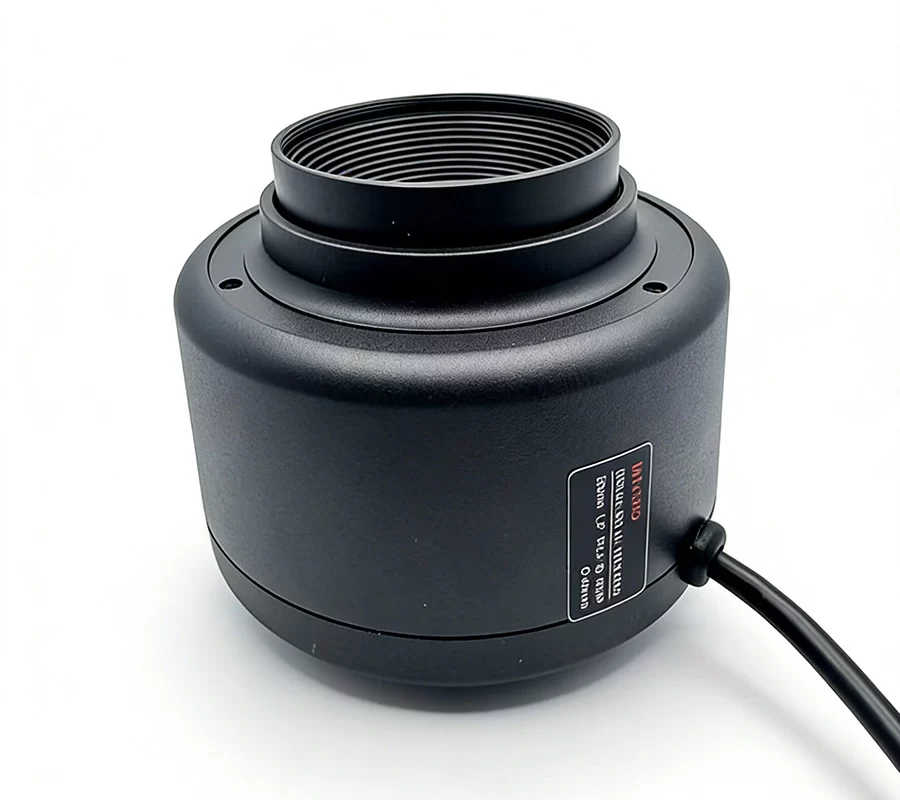
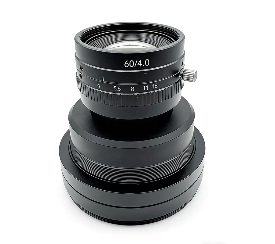
16K-3.5μm 60mm M72 Line-Scan Lens, Ultra-Low Distortion for 16K 3.5μm Line Scan Camera
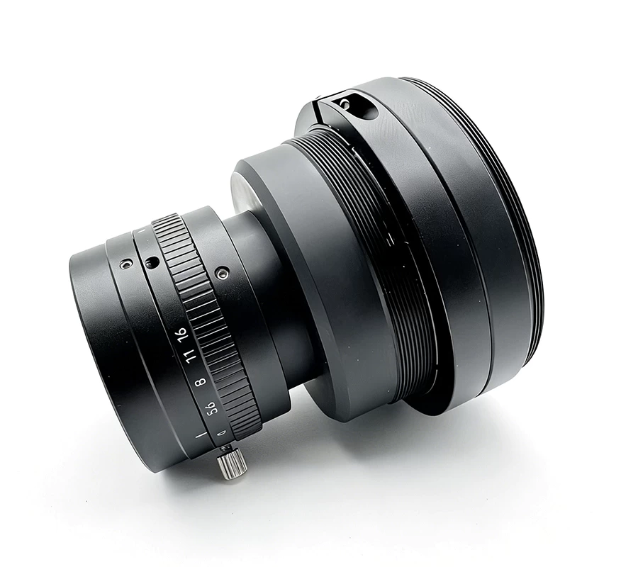
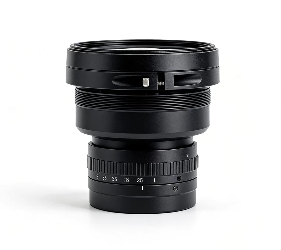
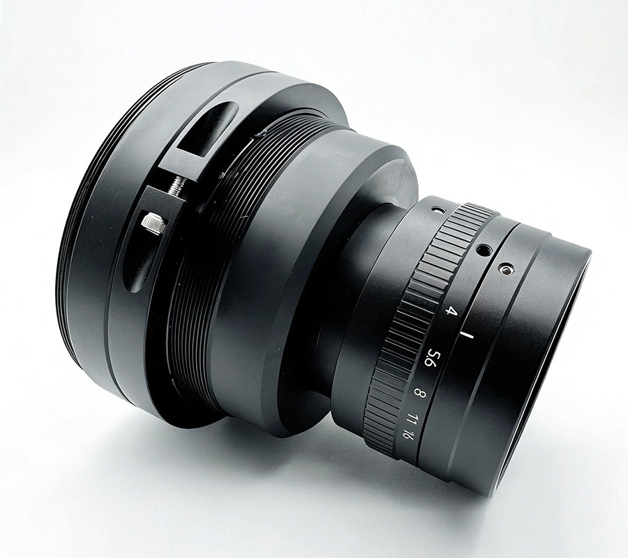
Specification of High-Resolution Line Scan Lens for 16K 3.5μm Line-scan Camera
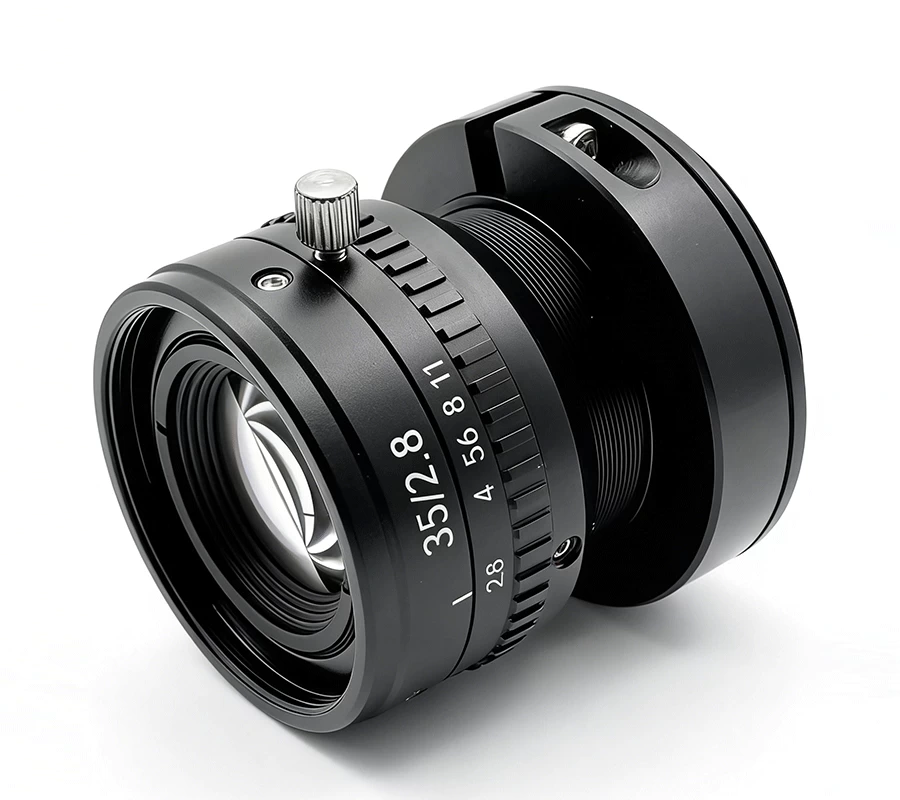
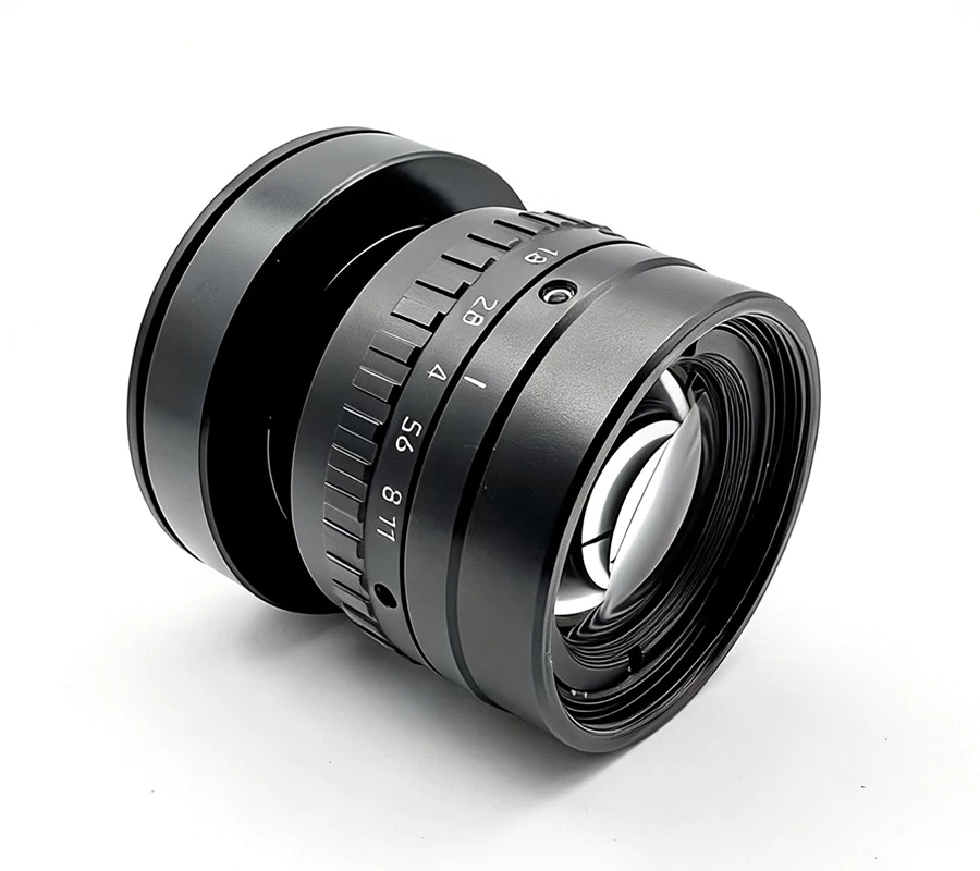
This high-performance industrial linear scanning lens is specifically engineered for 16K-resolution linear array sensors with a pixel pitch of 3.5 μm. Featuring a 60 mm focal length and an M72×1.0 standard flange interface, the optical design is rigorously optimized for linear array cameras equipped with a 57.6 mm sensor length and 3.5 μm pixels. The lens delivers a large effective image circle of Φ58 mm—fully covering the entire sensor—and achieves exceptional modulation transfer function (MTF) performance across the entire field of view. Geometric distortion is controlled to less than 0.02% (radial, absolute value), well below one pixel, while relative illumination uniformity exceeds 94% along the full scan line (±3% fluctuation). These attributes collectively ensure consistent spatial fidelity, micron-level resolution stability from center to edge, and geometric accuracy under dynamic, high-speed imaging conditions—thereby satisfying the stringent requirements of precision machine vision inspection for measurement reliability and imaging repeatability. The lens is widely deployed in wide-format, continuous online inspection and high-accuracy dimensional metrology applications across lithium battery manufacturing, printed circuit board (PCB) production, flat panel display (FPD) fabrication, optical film processing, printing and packaging, and photovoltaic module assembly.
Key technical specifications and performance advantages:
1. Pixel-level optical optimization for 16K × 3.5 μm sensors
The MTF response remains uniformly high across the full field of view, with negligible degradation at the edges. This ensures diffraction-limited resolution on every scanning line, eliminates edge blur and detail attenuation, and enables reliable micron-scale defect detection and quantitative morphological analysis.
2. Large Φ58 mm image circle with superior illumination uniformity
The image circle precisely matches the active length of the 16K linear sensor. Illumination variation along the scan line is limited to ≤ ±3%, effectively suppressing vignetting at both ends and minimizing the computational overhead and systematic error associated with brightness correction algorithms.
3. Ultra-low radial distortion (< 0.02%)
Distortion is maintained at sub-pixel levels across the entire field, preserving spatial integrity during high-speed scanning of wide-area substrates—including metal strips, electrode rolls, and flexible webs—thus preventing measurement bias, dimensional misregistration, and positional drift.
4. Robust M72×1.0 mechanical interface with dual-locking controls
The precision-machined threaded flange provides high structural rigidity and outstanding vibration resistance. Both the focus and aperture rings incorporate independent locking mechanisms, mitigating parameter drift induced by high-frequency mechanical vibrations in industrial environments and ensuring long-term imaging stability during uninterrupted operation.
5. Broadband anti-reflection coating (400–1000 nm)
A multi-layer vacuum-deposited coating achieves average transmittance > 95% across the visible and near-infrared spectrum. This significantly suppresses stray light, ghost images, and flare—ensuring stable, high-contrast imaging under diverse illumination sources, including white LED, halogen, and 850 nm NIR lighting.
6. Flexible working distance and scalable magnification
The 60 mm focal length supports a practical working distance range of 150–400 mm, offering an optimal balance between depth of field and resolution. By fine-tuning object distance, users can dynamically adapt the field of view and resolution trade-off to match varying inspection widths—enabling simultaneous optimization of throughput efficiency and fine-detail capture capability.
Typical application domains:
• PCB manufacturing: inspection of etched trace integrity, copper foil continuity, solder mask coverage uniformity, and detection of micro-vias, short circuits, and bridging defects;
• FPD fabrication: identification of surface anomalies—including scratches, particles, bubbles, and Mura non-uniformities—on glass substrates, color filters, polarizers, and OCA adhesive layers;
• Lithium battery electrode production: assessment of edge profile fidelity, coating thickness consistency, dry cracking, active-material shedding, separator porosity, and foreign-object contamination;
• Roll-to-roll web processing: real-time monitoring of lateral alignment deviation, color registration, contaminant spots, tape breaks, and surface defects across paper, BOPP/BOPET films, non-wovens, and printed materials;
• Photovoltaic module manufacturing: detection of silicon wafer micro-cracks and chipping, evaluation of thin-film uniformity (e.g., CIGS, perovskite, or CaTiO₃), and mapping of defect density distribution;
• High-precision online metrology: real-time measurement of width, thickness, contour geometry, and positional coordinates for wide-format materials—including metallic foils, composite laminates, and flexible electronics substrates.