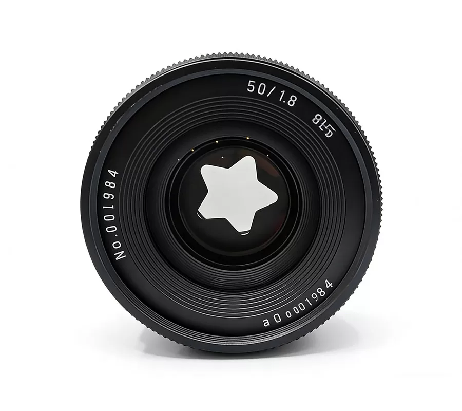
Every machine vision system stands or falls on its optics.
You can have the fastest camera, the most sophisticated algorithm, and the most precise motion stage — but if the lens cannot deliver a clean, well-resolved image to the sensor, none of it matters. The lens is the gateway between the physical world and your digital decision.
Choosing the right lens is not about picking the most expensive one. It is about matching four parameters to your application.
Key takeaways
• Four variables decide the selection: working distance, sensor format / image circle, Nyquist matching, spectral range. Aperture, distortion and mechanics are secondary choices made after these four are fixed.
• “5-megapixel lens” is a meaningless label. What matters is MTF at your sensor’s Nyquist frequency across your image circle — the same lens can be adequate on one sensor and unusable on another.
• Compute resolution in two steps: sensor Nyquist f_N = 1000/(2p), then back out magnification from “pixels per feature.” Collapsing them into one formula underestimates the requirement by 2–4.5×.
• Coatings buy transmission and ghost control — nothing else. They cannot beat the diffraction limit or correct design aberrations. A supplier without measured curves has not given you a specification.
The four parameters that matter
• Working Distance (WD). The space between the front of the lens and the object you are inspecting. Consider lighting room, protective windows, part-handler clearance and physical fit — and keep a 10–20% margin.
• Sensor Format / Image Circle. The lens must project an image large enough to cover your sensor, or the corners go dark and soft — unrecoverable in software. Common formats (nominal optical-format diagonals): 1/2.5″ (7.2 mm), 1/2″ (8 mm), 1/1.8″ (8.9 mm), 2/3″ (11 mm), 1″ (16 mm), 4/3″ (21.6 mm), 1.1″ (17.6 mm), APS-C (28.1 mm), full frame (43.3 mm). Note that 4/3″ is often quoted as 22.5 mm — that is the legacy vidicon figure; the industrial area-sensor diagonal is 21.6 mm (17.3 × 13.0 mm). Get the format wrong and you get the image circle wrong.
• Resolution Target. Do this in two steps rather than one combined formula.
Step one, sensor side: Nyquist frequency f_N = 1000 / (2p), with p the pixel pitch in µm. A 2.5 µm sensor gives 200 lp/mm — the frequency at which the lens must still carry usable MTF.
Step two, object side: if the smallest feature s must span at least p_x pixels (typically 2–3), the required magnification is m ≥ p_x·p/s, and the equivalent object-space requirement is 500·p_x/s (lp/mm).
Worked example: 100 µm feature, 3 pixels per feature, 2.5 µm pixels → m ≥ 0.075 and 15 lp/mm object-space. The widely copied formula “1000 ÷ (feature × pixels-per-feature)” is wrong: it is dimensionally inconsistent and returns 3.3 lp/mm here — 4.5× below the real requirement, which quietly spends your margin before you start.
• Spectral Range. This drives coating and glass requirements:
• Visible-light inspection: 400–700 nm — standard AR coating
• NIR applications: 700–1100 nm — AR-NIR or broadband coating required
• SWIR: 900–1700 nm (InGaAs detectors; the water absorption band sits near 1450 nm) — what you change is the coating, not the glass. N-BK7 transmits fully across 1350–1550 nm (effective window to 2.1–2.5 µm), as does fused silica; you only need different materials above 2.5 µm. Three things actually change: (1) a coating optimized only for 400–700 nm climbs to several percent per surface across 900–1700 nm — do not confuse that with reflection at the 940 nm end, where our own NIR-specified stack measures ≤1% per surface; the two are different problems, so specify SWIR broadband AR; (2) standard UV-cure cement absorbs and fluoresces in this band, so cemented doublets become air-spaced or SWIR-grade; (3) the diffraction limit at 1.5 µm is only 1/2.7 of that at 550 nm, so the same f-number resolves less — do not port a visible design unchanged.
• Laser systems: single wavelength — narrowband AR, optimized for that wavelength
Band | Typical detector | Usable glass / material | What must change | Tunable-cell (liquid lens) usability |
|---|---|---|---|---|
250–400 nm UV | UV-enhanced CMOS, PMT | Fused silica, CaF₂, sapphire | Material + UV coating (N-BK7 cuts off here) | — |
400–700 nm visible | Si CMOS/CCD | N-BK7, crown/flint, lanthanum | — | ✔ usable |
700–1100 nm NIR | Si | Same (incl. 940 nm) | Coating → AR-NIR | ✔ usable at 850 nm; marginal at 940 nm |
900–1700 nm SWIR | InGaAs | N-BK7, fused silica still work | SWIR broadband coating; air-spaced or SWIR cement | ✘ degrades past 1.2 µm; essentially opaque at 1450 nm |
1.55–2.5 µm extended SWIR | Extended InGaAs | Same | Same | ✘ |
2.5–5 µm MWIR | InSb, MCT (cooled) | Silicon, sapphire, CaF₂ | Material + coating + cooling | ✘ |
8–14 µm LWIR | Microbolometer | Germanium, ZnSe, chalcogenide | Material + coating (Ge is opaque in SWIR — LWIR only) | ✘ |
The two cells most often confused are SWIR and LWIR: in SWIR the glass is still the same glass and you change the coating and the cement; and germanium is not a universal “IR glass” — it is opaque from 1.35–1.55 µm.
Before you start matching, three physical limits of optics are worth stating, because they mean no lens can deliver everything at once:
• Diffraction is the hard ceiling — and it can be calculated. The correct criterion is not “Airy disk diameter versus pixel size” but diffraction cut-off 1/(λN) versus Nyquist 1/(2p) at λ = 550 nm. The cut-off is 455 lp/mm at f/4, 325 at f/5.6, 227 at f/8 and 165 at f/11. So a 2.5 µm sensor (Nyquist 200) is fine to f/8 and only starts losing real resolution at f/11, while a 2 µm sensor (Nyquist 250) drops below Nyquist already at f/8, leaving a usable window up to about f/5.6. Fifty megapixels does not automatically yield fifty megapixels of usable resolution — that is what the figure actually means.
• Flange distance caps large formats. The C-mount flange focal distance is only 17.526 mm, leaving little room behind the mount; correcting edge aberrations on formats above 1.1″ — especially in short focal lengths — is genuinely demanding, and larger formats often require F-mount or proprietary mounts. For large-format wide lenses, judge corner MTF, not just the center.
• No single coating covers every spectrum — and the penalty has a magnitude. Specify AR-NIR (800–1000 nm) or a dual-band design and the penalty largely disappears: Josight measures ≤1% residual reflection per surface at 940 nm on its own broadband AR — about 2% across two surfaces — with batch-level traces to back it up. A coating that was only ever specified for 400–700 nm behaves differently: several percent per surface at 940 nm is common, which costs light and opens a ghost path. 940 nm is the workhorse wavelength of active illumination and sits near the silicon QE peak, which is why “visible lens on a 940 nm source” is one of the most common field failures. Ask for the measured curve at your wavelength, not a band-average number.
Matching lens type to inspection task
Inspection Task | Recommended Lens |
|---|---|
Surface defect detection (scratches, stains, cracks) | FA lens, large aperture |
Dimensional measurement (hole diameter, pitch, flatness) | Telecentric lens (TL) |
Web / continuous material (film, paper, textile) | Line scan lens (LS) + line scan camera |
Guidance / sorting / pick-and-place | FA zoom or fixed focal |
Large-area high-precision | Bi-telecentric or high-res LS |
Coating: the unsung hero
• AR coating: quote the pair, not one number in isolation. Josight specifies its visible broadband AR as Ravg ≤0.5% and Rmax ≤1.0% per surface (single side, stated angle of incidence and substrate). The pairing is deliberate: Ravg alone hides a bad wavelength tail, Rmax alone undervalues a good average, and quoting both is the only way the reader can compare against another supplier. For scale, a 400–700 nm broadband stack realistically reaches Ravg 0.3–0.5% per surface; stretch it to 380–1100 nm and it typically degrades to 0.8–1.5%. Always state which metric, single side or double side, at what AOI — a bare “≤0.5%” is not a specification.
• IR coating: Above 1100 nm you change the coating, not the glass. Specify the band, bandwidth and angle range, and ask for the measured reflection curve.
• Specialty coatings: Hydrophobic, metallic-reflective, narrowband.
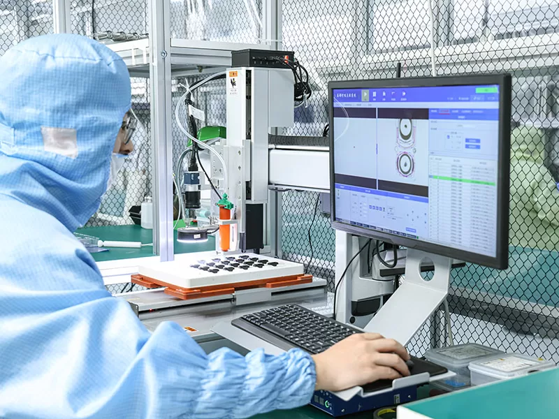
This is where an integrated manufacturer has an advantage: coatings applied on in-house vacuum coaters can be optimized for your exact band and co-developed with the optical design, rather than bought in from an unknown source. At Josight, ten vacuum coating systems operate on the same campus as our cold-processing and assembly lines, so the coating stack can iterate with the lens design and ship with batch-level measured transmission/reflection curves. One caveat: coating improves transmission and controls ghosting/stray light; it cannot beat the diffraction limit or correct design aberrations. A supplier that offers only a “broadband AR” label without measured curves is giving you marketing language, not an engineering specification.
Common selection mistakes (and how to avoid them)
Mistake 1: Ignoring illumination — specify lens and lighting together; telecentric backlight, coaxial light and ring light do not ask the same things of a lens.
Mistake 2: Over-specifying resolution — match the task, not the best spec sheet; resolution beyond sensor Nyquist is unusable but still on the invoice.
Mistake 3: Forgetting depth of field — confirm DOF against actual part geometry, not nominal height.
Mistake 4: Assuming one lens fits all — each station may need its own optimization.
Mistake 5: Trusting the “megapixel” label — what matters is the MTF-at-Nyquist curve over your image circle.
Mistake 6: Assuming a better coating raises resolution. Coatings improve transmission and ghost control; they do not move the diffraction limit and do not correct design aberrations. If resolution is short, the design is short.
Forward view: three trends rewriting the selection rules
Machine vision optics is not a static field. When specifying for today, keep these directions on your roadmap:
• 50-megapixel sensors go mainstream as pixels shrink. 1.1″ and larger formats with 2.x μm pixels are moving from high-end to mainstream, compounding the pressure on corner MTF, stray light and assembly decenter. “High-megapixel lens” labels become progressively meaningless; Nyquist-referenced curves become the baseline.
• Computational imaging and AI enter the selection loop. AI autofocus, scenario-based lens/camera recommendation, HDR and multi-frame fusion are already landing — but algorithms depend on a high-quality, stable front-end image, so optical consistency (per-unit MTF, batch stability) matters more, not less. Garbage in is still garbage out.
• Multispectral / hyperspectral and new imaging dimensions. Moving from monochrome and RGB to multispectral (material sorting, defect composition) and 3D (structured light, light field, ToF) means lenses must perform across wider bands or with specific phase behavior; coating and optical design must be considered from day one.
Practical advice: specify for today’s task, but ask whether your supplier’s optical platform has headroom — whether the same platform covers the next, larger sensor generation and supplies measured data in your band.
Next steps
Practical checklist before talking to a supplier:
☐ Sensor model and pixel pitch confirmed?
☐ Working distance range measured (with margin)?
☐ Smallest feature size and pixels-per-feature defined?
☐ Light source wavelength identified?
☐ Task type (detection vs. measurement) clarified?
FAQ
Q1: How many lp/mm does my lens need?
Two steps. (1) Sensor Nyquist f_N = 1000/(2p), with p in µm — 2.5 µm needs 200 lp/mm, 3.45 µm needs 145 lp/mm. (2) Object-space requirement = 500 × (pixels per feature) ÷ (feature size in µm) — a 100 µm feature at 3 pixels per feature is 15 lp/mm. Take whichever is stricter, then ask for MTF curves. Avoid the widely circulated “1000 ÷ (feature × pixels-per-feature)” formula: it under-estimates by 2–4.5×.
Q2: Can a 5-megapixel lens work on a 12-megapixel camera?
It will mount, but the rating means nothing. What decides usability is how much MTF the lens still delivers at your Nyquist frequency, not its nominal megapixel label. A 12 MP 1/1.8″ sensor (≈2.4 µm pixels) needs usable contrast near 208 lp/mm; a lens sold as “5 MP” is usually close to cut-off there. The only valid test is a field-resolved MTF curve over your image circle.
Q3: Why does SWIR need a different lens?
Mostly a different coating and cement, not different glass. N-BK7 and fused silica still transmit from 900–1700 nm, but a coating built only for the visible band climbs to several percent per surface across that range, and standard UV-cure cement absorbs and fluoresces. Separately, the diffraction limit at 1.5 µm is only 1/2.7 of that at 550 nm, so the same f-number resolves noticeably less — which is why SWIR systems usually run at smaller f-numbers.
Q4: How large a sensor can C-mount support?
4/3″ (21.6 mm diagonal) is effectively the practical ceiling. Two reasons: the 17.526 mm flange distance leaves very little room behind the mount for the rear group on short focal lengths, and the 1″-32 thread (25.4 mm, roughly 22–23 mm clear aperture) caps the usable image circle mechanically. Beyond that you move to F-mount, M42/M48, M58/M72 and larger. Always judge corner MTF on the format you will actually use.
Q5: Does a coating improve resolution?
No. A coating improves transmission and controls ghosting and stray light; it neither moves the diffraction limit nor corrects residual aberrations. A lens short of MTF stays short of MTF. Conversely, running a visible-band lens at 940 nm costs you light at the coating, and the amount depends entirely on how the stack was specified: our own broadband AR measures ≤1% per surface there (about 2% for two surfaces), while a stack designed only for 400–700 nm can reach several percent per surface. Either way it is a coating problem, not a resolution problem — keep the two discussions separate.
Need help matching a lens to your application?
Send us your sensor datasheet, working distance, what you are inspecting, and accuracy goal. We will recommend the right spec, provide MTF data at your wavelength and Nyquist frequency, and supply test samples.
Disclaimer
The information in this article is provided for general informational purposes only. Lens specifications, performance data and product availability are subject to change without notice. Actual performance may vary with application conditions, system configuration and environmental factors. Josight makes no warranties, express or implied, regarding the accuracy, completeness or suitability of the information herein. Readers should conduct their own testing and validation before making procurement decisions.